© Universität Bielefeld
The research group Physics of Supramolecular Systems and Surfaces is focused on the fabrication, characterization and application of functional nanomaterials with a emphasis on two-dimensional carbon and graphene.
The group pioneered the fabrication of carbon nanomembranes (CNMs) from cross-linked self-assembled monolayers. The group lays a strong effort on technological applications of CNMs and explores their use for electronics, photonics, biotechnology, and as tailored filter membranes for gas and liquid separation.
Our laboratory uses modern preparative and analytical tools: electron microscopes, photoelectron spectrometers, scanning probes and CVD systems. We also operate the first helium ion microscope (HIM) at a German university. Our HIM is used for high-resolution imaging and nanolithography with a focused He ion beam.
Surface Studies and Self-Assembled Monolayeres


Specific functionalization of surfaces is of crucial importance in the material sciences. In particular in nanotechnology, complex functionalizations are desired for an increasing number of applications, which will require the development of novel interface modification strategies. Examples are the functionalization of electrodes for organic electronics, the remote control of surface properties by optical switching, the setup of biomimetic or biologically relevant interfaces (cell recognition, differentiation of stem cells, and the colonization of technical surfaces by microorganisms) as well as coatings of implants.
The most promising strategies of such surface functionalization are based on self-assembled monolayers (SAMs). SAMs have not only turned out to be the model system for organic surfaces, but are of high relevance to both fundamental and applied research. Above all, they serve as a technology platform for the further development of nanotechnology.
SAMs have produced a number of innovative stimuli in materials sciences and are increasingly applied as a technology platform for the (further) development of nanotechnology. Examples are:
Functional coatings in organic electronics.
Carbon nanomembranes (CNMs) for sensors and bioengineering.
Control of protein affinity on surfaces for medical engineering.
Platform for highest-resolution (sub-10 nm) lithography.
Tribological coatings of nanomechanical components.
Owing to the unique combination of simple production and excellent structural properties, SAMs are particularly well suited as model systems for studying basic interface phenomena at both solid-gaseous and solid/liquid phase boundaries. SAMs have a small thickness which makes them accessible by classical electron spectroscopy methods. Practically all standard methods of surface analysis can be applied directly to these organic thin layers. Hence, the complete knowledge base established for metal and inorganic substrates in "Interface Sciences" can be applied, including diffraction methods. As a result SAMs are ideal to validate different types of theoretical approaches. Whereas thin polymer films, for example, also offer a large variety of options with regard to obtaining highly functional interfaces, they typically lack the high degree of perfections obtainable with SAMs. As a consequence, the application of diffraction methods is difficult and a reliable, direct validation of theoretical calculations is hampered for such systems.


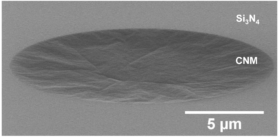
Carbon Nano Membranes (CNMs)


Helium Ion Micrograph of a CNM on copper grid.
Carbon Nano Membranes (CNMs) are similar to plastic foils, but only ~1 nanometer thick. CNMs are made by radiation induced cross-linking of surface bound organic molecules. CNMs can be chemically and biologically functionalized as well as transformed into graphene, thus providing a 2D-platform for applications.
From Monolayers to Nanomembranes
The starting point of CNM fabrication is a self-assembled monolayer (SAM) of aromatic molecules which are linked to a surface via a functional group. When the so-assembled molecules are exposed to radiation, one obtains a ~1 nm thick mechanically stable film of cross-linked carbon. The Gölzhäuser group is working with partners in Europe, the US and Japan on the characterization of these materials for electrical, optical and mechanical purposes, and towards applications of CNMs into new products.
CNM onto oxidized silicon, due to the interference contrast, the CNM is visible with the naked eye. It can be seen folding their colors. Bottom: Transmission electron micrograph of a CNM decorated with small gold particles. CNM forms in three steps. Lead compounds are bi- or terphenyls, which adsorb on a surface via a functional group. The SAMs are bombarded with electrons or extreme ultraviolet photons. This breaks intramolecular bonds and adjacent molecules form cross-links. A special method -developed in Bielefeld- allows CNMs to be transferred from one surface onto another, including materials and objects on which otherwise no SAMs form, such as grids for transmission electron microscopy. The transfer technique also allows the integration of CNMs into silicon chips or micro-structured surfaces
CNMs from different precurser molecules.
CNMs have significant potential for technological applications. CNM based products include support membranes for electron microscopy of nanometer scale objects, where the support structure is often thicker than the actual nano-object, which results in a poor image quality. The CNMs, however, are thinner than most nano-objects, which improves the image contrast significantly. In addition to the thickness, the chemical functionalities of the two sides of the CNM can be tailored by the choice of suitable molecules. By selecting the irradiation parameters, the degree of cross-linking and thus the elasticity of the CNM can be tuned. In summary, CNMs are a new class of materials with interesting properties that lead to innovative products in many fields


Mechanics of CNMs
To study the elastic and viscoelastic behaviors of freestanding CNMs, we developed a method -AFM bulge test- that uses an atomic force microscope to measure the displacement of a membrane bulging due to a pressure difference. Depending on the type of precursor molecules, Young's modulus of CNMs can be tailored within the range of 10 to 20 GPa, which is about 50- to 100-fold smaller than that of graphene monolayer (~1 TPa), but slightly higher than the upper bound of polymeric membranes. A correlation between the rigidity of the precursor molecules and the macroscopic mechanical stiffness of CNMs is thus revealed. Our setup is capable of determining a strain rate as low as 10-8s-1, and the creep rates of CNMs are in a range of 10-6 s-1 at RT. The Creep behavior of CNMs appears to be stress-dependent and thermally activated, which can partially recover in the absence of an external load.


Helium Ion Microscopy (HIM)


The Zeiss Orion Plus Helium Ion Microscope in Bielefeld
A Helium Ion Microscope (HIM) is capable to image conductive as well as insulating samples without special treatment, in particular it allows imaging of unstained biomaterials and cell surfaces. HIM has the potential to become the routine microscopy for material science and nanotechnology, as well as in life science and biotechnology.
We are interested in all questions ranging from image formation and contrast mechanisms to materials imaging, bioimaging and lithography.
Further information about HIM is provided in our article ‘Das Heliumionen-Mikroskop: Mikroskopie mit geladenen Teilchen’ ( [Opens external link in new window] link to journal).
Free-standing CNMs
A collection of different CNMs on hexagonal copper grids is presented, exhibiting the different types of features that are visible in HIM images. From these images, one intuitively obtains an impression of the detailed shape of the copper grid and the CNM on top. In a) larger folds on the upper side of the image and one rupture in the centre are visible. b) is an example of a membrane rolling up at a rupture, showing the high flexibility of CNMs. Small folds like those in c) are frequently observed, while wrinkling of the freestanding membrane (d) is less often observed.


Freestanding Carbon Nano Membranes on copper grid (a-c) and graphene (d).
Soot from ethylene flames
Morphological variations of nascent soot collected from the ethylene C3 flame at heights of 0.5, 0.8 and 1.2 cm and imaged by HIM, showing representative primary and aggregate structures. Particles shown in the hexagons are in the apparent size range of 4-8 nm; those in the squares are 14-18 nm. Particles shown in the circles are apparent aggregates.


CVD grown films of iron and cobalt mixed oxides.
Mammalian cells
In specimens sputter coated with gold (top row) with a standard thickness of approx. 10 nm, the cell membrane is covered with clustered gold, masking the true cell surface. The effective charge compensation in HIM allows a high resolution inspection of uncoated cell surface in the native state (bottom row).

