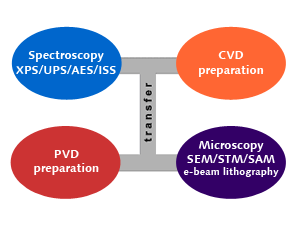
Equipment

Laboratory for Preparation and Characterization of Nanostructures
Surface-Spectroscopy
XPS
X-ray Photoelectron Spectroscopy (XPS) is a powerful analytical technique used to study the surface chemistry of materials. By irradiating a material with X-rays, XPS measures the kinetic energy and number of electrons that escape from the top layers of the sample. This provides detailed information about the elemental composition, chemical state, and electronic state of the elements present. Its ability to provide quantitative and qualitative data with high surface sensitivity makes it an invaluable tool for understanding material properties and interactions at the atomic level.
Thanks to an integrated flood source the analysis of insulating materials and samples that are prone to charging is possible. The flood source emits low-energy electrons or ions to compensate for the positive charge that builds up on the sample surface during analysis. This charge neutralization ensures that the kinetic energy of emitted photoelectrons is accurately measured, thereby providing reliable data on the elemental composition, chemical states, and electronic structure of the sample.
ARXPS
ARXPS stands for Angle-Resolved X-ray Photoelectron Spectroscopy. It is a variation of X-ray Photoelectron Spectroscopy (XPS) that provides additional information about the depth distribution of elements and chemical states within a sample. By varying the angle at which the photoelectrons are detected relative to the sample surface, ARXPS can distinguish between surface and subsurface layers. This technique allows for the non-destructive analysis of thin films and layered structures, providing insights into the chemical composition and thickness of each layer.
UPS
UPS complements XPS by providing additional information about the valence band structure and work function. Similar to X-ray Photoelectron Spectroscopy (XPS), UPS involves the emission of electrons from a material's surface; however, it uses ultraviolet light to achieve this. Together, they provide a comprehensive understanding of both the surface chemistry and electronic characteristics of materials.
AES
Auger Electron Spectroscopy (AES) is another technique used to explore the surface composition and chemical states of materials. By inducing the emission of Auger electrons through electron bombardment, AES provides information about the elemental composition and chemical environment of the top few nanometers of a material's surface. Thus, complementing these methods by offering superior spatial resolution and sensitivity to surface chemistry.
ISS
Ion Scattering Spectroscopy (ISS) is a precise analytical technique used to investigate the surface composition and structure of materials. By directing a beam of noble gas ions at a material’s surface and analyzing the scattered ions, ISS provides detailed information about the elemental composition of the outermost atomic layers. This makes ISS particularly valuable for the study of thin films, coatings, and surface modifications. ISS excels in analyzing the arrangement and composition of atoms on the surface, providing critical insights into surface phenomena such as catalysis and corrosion.


Microscopy
SEM
A Scanning Electron Microscope (SEM) operates by scanning a finely focused electron beam across the sample surface, generating signals that reveal detailed topographical and compositional information. The in-lens detector provides exceptional surface sensitivity and high-resolution imaging, making it ideal for observing fine nanoscale features. The Everhart–Thornley detector excels at capturing secondary electrons with strong topographic contrast, offering intuitive three-dimensional visualization of surface morphology. This combination of detectors ensures versatile and high-quality imaging for a wide range of applications in materials science, nanotechnology, and biological research.
SAM
For detailed mapping of elemental composition at the nanometer scale, the system is equipped wit a Scanning Auger Microscope (SAM). The SAM scans also the sample with a electron beam but detects auger electrons. While SEM provides excellent topographical and morphological information, SAM complements it by offering spatially resolved chemical analysis.
VT-STM
A Scanning Tunneling Microscope (STM) is an instrument used for imaging surfaces at the atomic scale. STM operates by bringing a sharp conductive tip very close to a sample surface. When a voltage is applied, a tunneling current is produced by electrons that tunnel between the tip and the sample. The STM generates highly detailed, three-dimensional images with atomic resolution by measuring the tunneling current as the tip scans across the surface. In addition our STM is capable of scanning at variable temperatures, enabling the study of temperature-dependent surface phenomena.
Preparation
PVD
In physical vapor deposition (PVD), the material to be deposited – the evaporant – is heated until it evaporates. This evaporant can be supplied in the form of a bar, rod, or placed in a crucible. Electron bombardment heating is commonly used to rapidly increase the temperature of the evaporant. As the temperature rises, the material transitions into the vapor phase and deposits as a thin film onto the target substrate.
Sputtering
Sputtering is an essential technique used in sample preparation to achieve clean and well-defined surfaces. In this process, a sample is bombarded with energetic ions—most commonly argon ions—in a vacuum environment. The ion bombardment effectively removes surface contaminants and thin layers of material, resulting in a pristine surface that is ideal for subsequent analysis or processing.
Sample heating
After sputtering, annealing the sample is necessary to further improve surface quality and remove defects introduced during ion bombardment. In our laboratory, this is achieved by direct heating of a tungsten filament in close proximity to the sample.
Low Energy Electron Irradiation
Low Energy Electron Irradiation is a technique in which materials are exposed to a controlled beam of electrons with energies typically ranging from a few electronvolts (eV) up to several kiloelectronvolts (keV). This method is widely used to modify surface properties, induce chemical reactions, or investigate radiation effects in various materials.


Helium Ion Microscope Orion from Zeiss
ELPHY MultiBeam Pattern Generator from Raith https://raith.com/product/elphy/


AFM
Atomic Force Microscopy (AFM) is a high-resolution imaging technique used to analyze the surface topography of materials at the nanometer scale. AFM operates by scanning a sharp tip attached to a flexible cantilever across the sample surface. As the tip interacts with the surface, forces between the tip and the sample cause deflections of the cantilever, which are measured with high sensitivity. These deflections are used to construct detailed three-dimensional images of the surface. In addition to imaging, AFM can also measure local mechanical properties


IRRAS
Infrared Reflection Absorption Spectroscopy (IRRAS) is a surface-sensitive analytical technique used to investigate the molecular structure and composition of thin films and surfaces. By directing infrared light at a grazing angle onto a sample and measuring the reflected light, IRRAS provides detailed information about vibrational modes of molecules adsorbed on reflective surfaces, such as metals. This technique is particularly suited for studying organic and biological monolayers, self-assembled films, and surface reactions.
ATR-IR
Attenuated Total Reflection Spectroscopy (ATR) is an infrared spectroscopic technique that enables the analysis of surface and thin film properties with minimal sample preparation. In ATR, an infrared beam is directed into a crystal with a high refractive index. When the beam reflects internally at the interface with the sample, it generates an evanescent wave that penetrates only a few micrometers into the sample. This allows for the collection of absorption spectra from the sample surface or thin layers.

